Automated capture process simplifying emission capture and overlays.
Advanced filter process for removal of hot pixel and cosmic ray noise.
Calibration tables matched to the camera for unsurpassed sensitivity and clarity.
Color overlays and multiple window views for emission comparison.
Video feed out allows interface to existing probe station software.
High Sensitivity Extended IR Sensor in the visible to NIR range.
13 bit Analog/ Digital hybrid enabling real-time imaging capability.
Excellent anti-blooming characteristics.
Selectable 8 bit readout control across 13 bit dynamic range.
High resolution and low dark current.
Air cooled with typical 60° C Differential resulting in -35 to -45° C at the sensor
Detector: Indium Gallium Arsenide (InGaAs)
Array Format: 320 (H) x 256 (V) Focal Plane Array
Pixel Size: 30 x 30 microns
Spectral Response: 900 to 1700 nanometers
QE: 80-85%
Optical Fill Factor: >90%
Thermal Stabilization: Thermoelectric
Window Material: BK-7 Optical Glass
Digital Data Real-time, 12-bit, Parallel
Integration Type: Snapshot Mode or Software Paced Sequential Readout
Integration Time: Range 1 µsec to 60 minutes
Sensitivity: NEI <1×10¹⁰ ph/cm2/sec
Damage Threshold: >1 W/cm2
Time to Initial Image: 30 sec @ 25°C ambient; ≤ 1 sec, not temperature dependent. Full stabilization <5 minutes.
Cooling Method: Multistage TEC
Power Dissipation: 12W typical
Power Connector: Custom controlled via emission software
No LN2 dewars!
How does FMI works?
This technique involves coating a sample surface with a special Thermal sensitive fluorescent rare earth-based thin film dye that,
upon exposure to UV light, Emits temperature-dependent fluorescence
at 612nm.
Because of its temperature, emission/absorption characteristics,
availability, and other qualities.
More specifically, it has the best fit for temperature dependent
fluorescence quantum yield in the temperature range near room temperature.
The PITS‑2 Thermal Imaging System is a powerful failure‑analysis solution designed to accurately detect hotspots caused by short defects on device chips.
With the rapid growth of new energy vehicles, the adoption of SiC chips and IGBT modules has increased significantly, driving a greater need for advanced and reliable failure‑analysis tools.
Designed to meet these evolving demands, the PTIS‑2 thermal imaging system delivers enhanced diagnostic capability, including the ability to detect low‑current hotspots using our advanced lock‑in thermography.
This ensures precise, dependable analysis for today’s high‑performance power devices
The probe station supports testing across a wide range of samples, including decapsulated devices, bare chips, and full wafers.
An integrated thermal stage ensures optimal conditions for high‑quality thermal imaging during testing.
With four IR lenses and an optical lens, the system enables automatic lens switching for maximum flexibility and ease of use.
Advanced lock‑in thermography technology allows reliable detection of low‑power hotspots and low‑resistance shorts, delivering precise and dependable failure analysis results.
Features:

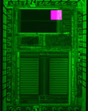
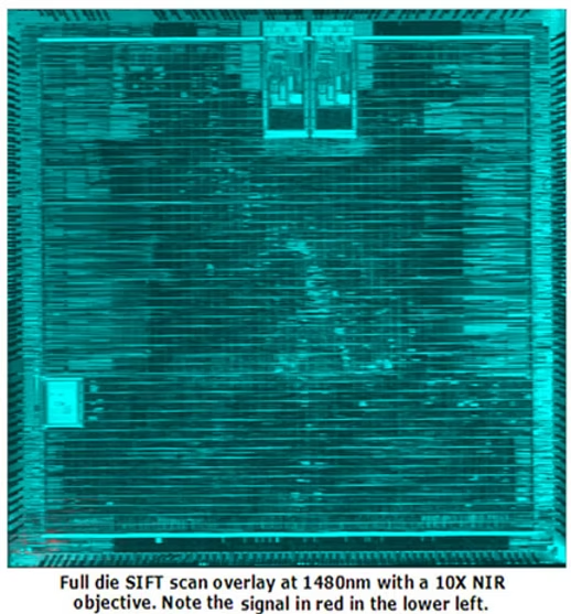
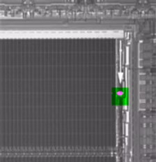
SIFT enables comprehensive analysis across multiple stimuli to quickly identify speed variations, faults, and parametric differences in silicon.
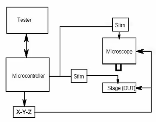
At the core of the SIFT technique is the intentional stimulation of devices using external inputs, with results compared against reference parts or timing and voltage sensitivities for precise insight.
Seamless synchronous interfacing allows compatibility with virtually any tester—no wiring changes or program modifications required.
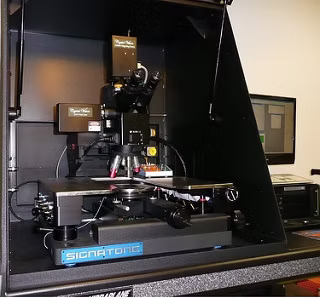
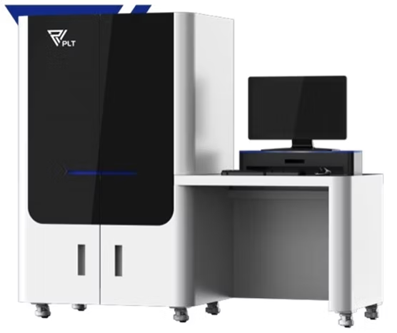
The system can be configured on either a motorized probe station or a portable microscope stand, making it ideal for both bench‑top analysis and test‑head applications.
Unlike traditional laser scanning microscope systems, the SIFT scanner features a straightforward, robust design without complex optical assemblies.
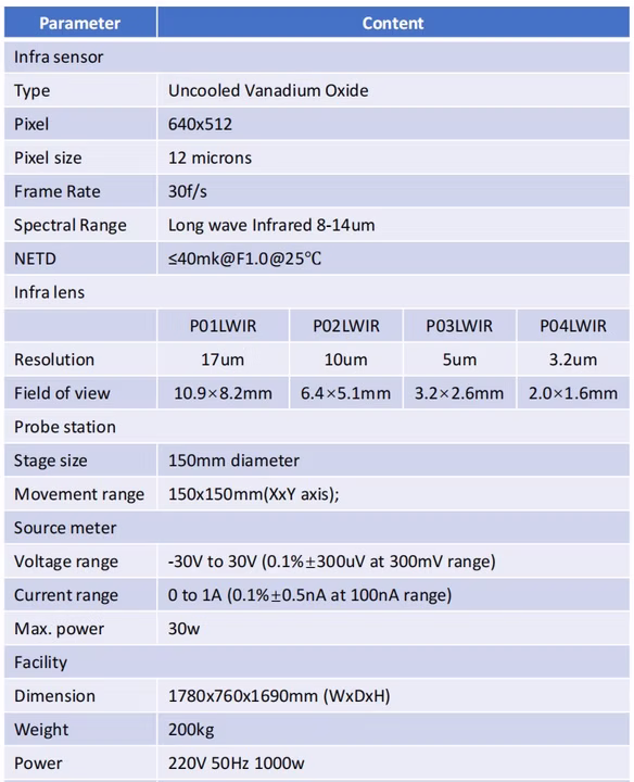
Its stepper‑based scanning approach enables DUT scan areas ranging from microns up to 300 mm or more, allowing entire boards, packages, and individual die to be analyzed with ease and flexibility.
Spot = 100 microns
126 test loops for 9×14 area Test time = 500 msec/loop
Spot = 50 microns
Radiant Optronics
Store Manager
Radiant Optronics
Hey, how can I help you today?